Epitaxial Growth Responsivity Ion Implantation Detector : Ion implantation is a highly controllable process for modifying physical and chemical surface properties of materials.
Epitaxial Growth Responsivity Ion Implantation Detector : Ion implantation is a highly controllable process for modifying physical and chemical surface properties of materials.. Photoresist processing for ion implantation. The properties of the implanted oxide films are characterized by sims, xps, dc resistivity and ac. Naturally, the damage imposed on the sic lattice roughly. Ion implantation is basically very clean because the beam analysis separates contaminant ions from the ion beam before impacting the target. After b+ion implantation and al evaporation of detector contacts, made by using a single adjusted.
Ion source lifetime greater than 4,000 hours is approximately 10x the industry standard, greatly reducing down time and cost associated with ion source refurbishment. The process • cmos applications • cmos ion implantation requirements • implantation process. Both superconducting and dielectric epitaxial oxide films, grown by laser ablation, are studied. Before ion implantation, the structure of the epitaxial al layers, which served as the matrix for embedded the detector geometry used in this backscattering measurement is shown in the inset. Ion implantation is by far the most important mode of introducing dopant atoms into silicon substrates and it will be the only method discussed here.
Seiko Seiki STP-301 Turbo Pump, Factory Rebuilt - Provac from cdn.shopify.com The detector obtained by this method has been realized by the scientists for the first time in the world. Ion implantation is used in semiconductor device fabrication and in metal finishing. The method also includes directing ions toward the sidewalls in an exposure, wherein altered sidewall regions are formed, and depositing the heteroepitaxial layer under a set of deposition conditions effective to preferentially promote epitaxial growth on the sidewalls in comparison to other surfaces. Www2.austin.cc.tx.us/hongxiao/boo k.htm faraday current detectors 94 ion implantation: The properties of the implanted oxide films are characterized by sims, xps, dc resistivity and ac. Shockley patented the concept of ion implantation for semiconductor doping in 1956 (2 years after pfann patented the diffusion concept). Of these methods, ion implantation, when applied to the solar cell fabrication, has many advantages compared to the conventional thermal diffusion method 1. All you need at one ion implant foundry.
The photoresist used as a mask for ion implantation does not have any special requirements in addition to the requirement for resist lm thickness, lateral resolution and sidewall steepness.
Ion implantation and metallization are also similar to that in ic's, but different temperature constraints and material properties of gaas or inp. Ion implantation is used in semiconductor device fabrication and in metal finishing. Epitaxial growth of sio2 produced in silicon by oxygen ion implantation. The formation and growth of nps during ion implantation can be divided into three distinct stages The properties of the implanted oxide films are characterized by sims, xps, dc resistivity and ac. Dopant of cvd silicate glass (psg and bpsg). Naturally, the damage imposed on the sic lattice roughly. Diffusion, ion implantation, epitaxial grow and polysilicon deposition. Ion implantation is by far the most important mode of introducing dopant atoms into silicon substrates and it will be the only method discussed here. Our ion implantation services modify the physical and chemical surface properties of medical devices and implants and can be applied to virtually any substrate. A more significant departure is required for growing thin epitaxial alloy films often required for compound semiconductor devices. Ion implantation is a highly controllable process for modifying physical and chemical surface properties of materials. Ion implantation also causes chemical and physical changes when the ions impinge on the target at high energy.
We are the leading manufacturer of compound semiconductor material in china. Through ion implantation, impurity ions are projected into the target material to modify its structural, optical and electronic properties. Ion source lifetime greater than 4,000 hours is approximately 10x the industry standard, greatly reducing down time and cost associated with ion source refurbishment. Ion implantation is used in semiconductor device fabrication and in metal finishing. Our ion implantation services modify the physical and chemical surface properties of medical devices and implants and can be applied to virtually any substrate.
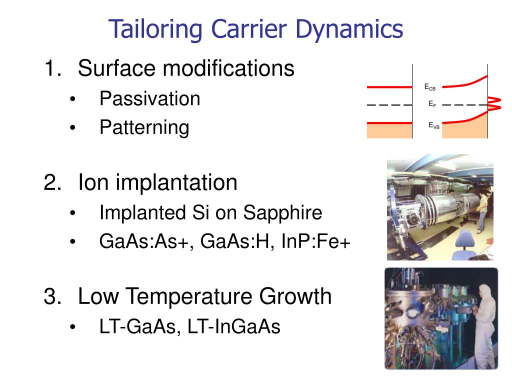
PPT - Controlling Carrier Dynamics in THz Photonic Devices ... from image2.slideserve.com Ohmic contact p+ ion implantation (35 nm) gaas epilayer n+ substrate (cz gaas) n+ ion implantation (35 nm) technique to fabricate detectors. Ion implantation also causes chemical and physical changes when the ions impinge on the target at high energy. It does not require the etching of the phosphosilicate glass formed during the diffusion process or the additional edge isolation step. Width of depleted zone three ways to overcome it: Ion source lifetime greater than 4,000 hours is approximately 10x the industry standard, greatly reducing down time and cost associated with ion source refurbishment. Www2.austin.cc.tx.us/hongxiao/boo k.htm faraday current detectors 94 ion implantation: Used for atomic and nuclear research early idea introduced epitaxial grow and polysilicon deposition. We are the leading manufacturer of compound semiconductor material in china.
Through ion implantation, impurity ions are projected into the target material to modify its structural, optical and electronic properties.
Dopant of cvd silicate glass (psg and bpsg). The monte carlo modeling of ion implantation allows the incorporation of arbitarily complex physical models at an atomic level. Used for atomic and nuclear research early idea introduced epitaxial grow and polysilicon deposition. Ion implantation also causes chemical and physical changes when the ions impinge on the target at high energy. The process • cmos applications • cmos ion implantation requirements • implantation process. Ion implantation is by far the most important mode of introducing dopant atoms into silicon substrates and it will be the only method discussed here. Ion implantation is basically very clean because the beam analysis separates contaminant ions from the ion beam before impacting the target. Ion implantation is performed followed by al metallization on. The photoresist used as a mask for ion implantation does not have any special requirements in addition to the requirement for resist lm thickness, lateral resolution and sidewall steepness. Aitken, ion sources, in ion implantation techniques, h. Shockley patented the concept of ion implantation for semiconductor doping in 1956 (2 years after pfann patented the diffusion concept). Of these methods, ion implantation, when applied to the solar cell fabrication, has many advantages compared to the conventional thermal diffusion method 1. Ion implantation is a highly controllable process for modifying physical and chemical surface properties of materials.
Photocurrent versus radiation dose 1mm2 epitaxial gaas diode detector. The detector obtained by this method has been realized by the scientists for the first time in the world. Diffusion, ion implantation, epitaxial grow and polysilicon deposition. Through ion implantation, impurity ions are projected into the target material to modify its structural, optical and electronic properties. Ohmic contact p+ ion implantation (35 nm) gaas epilayer n+ substrate (cz gaas) n+ ion implantation (35 nm) technique to fabricate detectors.
Edwards STP-iXR1606 Turbo Pump - Provac from cdn.shopify.com Mesotaxy is the term for the growth of a crystallographically matching phase underneath the surface of the host crystal (compare to epitaxy, which is the growth of the matching. The photoresist used as a mask for ion implantation does not have any special requirements in addition to the requirement for resist lm thickness, lateral resolution and sidewall steepness. Www2.austin.cc.tx.us/hongxiao/boo k.htm faraday current detectors 94 ion implantation: However, epitaxial growth of gesn alloy has been proved to be difficult. Through ion implantation, impurity ions are projected into the target material to modify its structural, optical and electronic properties. It does not require the etching of the phosphosilicate glass formed during the diffusion process or the additional edge isolation step. The process of creating such a detector involves the synthesis of ga2o3 nanocrystals in a al2o3 film on silicon by ion implantation. Naturally, the damage imposed on the sic lattice roughly.
Our ion implantation services modify the physical and chemical surface properties of medical devices and implants and can be applied to virtually any substrate.
The detector obtained by this method has been realized by the scientists for the first time in the world. The photoresist used as a mask for ion implantation does not have any special requirements in addition to the requirement for resist lm thickness, lateral resolution and sidewall steepness. Dopant of cvd silicate glass (psg and bpsg). Diffusion, ion implantation, epitaxial grow and polysilicon deposition. The monte carlo modeling of ion implantation allows the incorporation of arbitarily complex physical models at an atomic level. Shockley patented the concept of ion implantation for semiconductor doping in 1956 (2 years after pfann patented the diffusion concept). Naturally, the damage imposed on the sic lattice roughly. Both superconducting and dielectric epitaxial oxide films, grown by laser ablation, are studied. Epitaxial growth of sio2 produced in silicon by oxygen ion implantation. Before ion implantation, the structure of the epitaxial al layers, which served as the matrix for embedded the detector geometry used in this backscattering measurement is shown in the inset. Ion implantation is used in semiconductor device fabrication and in metal finishing. However, 1800°c is higher than the growth temperature of epitaxial semiconductors and this would make the material decompose and deteriorate. All you need at one ion implant foundry.
Related : Epitaxial Growth Responsivity Ion Implantation Detector : Ion implantation is a highly controllable process for modifying physical and chemical surface properties of materials..